Table of Contents
Intro

Last year I came across a video on RedNote(小红书), posted by user “老车有毒” in which he converted a 1970s AM General bus into a mobile coffee shop. He removed some parts from the bus, including seats, interior parts and rollsigns for sale. I got in touch with him and purchased the set of rollsigns.


The Bus
The bus is an AM General Metropolitan Series 10240B-8 (Flyer D800), serial number 10240B001176. It has Detroit Diesel 8V71N engine and Allison V730 transmission.
According to CPTDB Wiki It served as Denver Regional RTD bus number 4672 before being sold to Community Transit in Lynnwood, Washington in 1990 and became bus number 308.
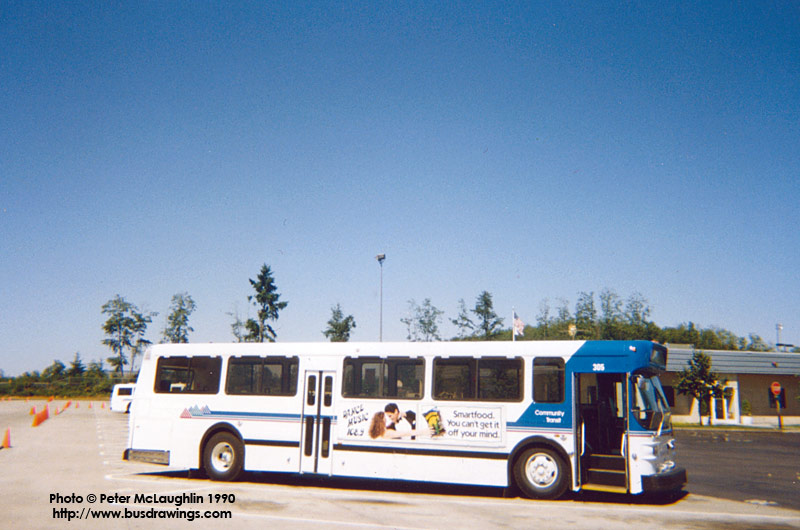
What happened next may not be completely precise and is just what I know. When the AMGs were retired one (or some) of the buses were sold to some southeast Asia country. It was unloaded at the Port of Tianjin(天津港), China but it was never loaded again due to customs. After staying at 天津港 for more than 10 years, in 2024 it was sold to “a private buyer” for RMB 80,000 (about USD 12,000).
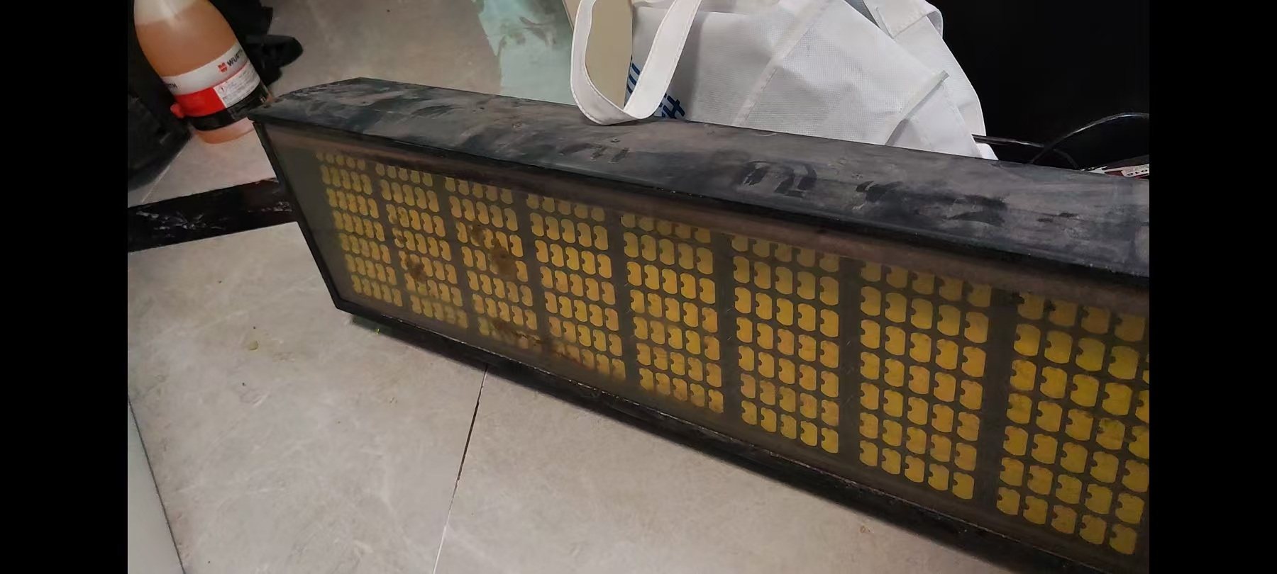
Here’s a screenshot of the current look of bus 308.


If you would like to know what happened to the bus you can follow “老车有毒” on 小红书(Rednote) or 抖音(Douyin).
The Displays
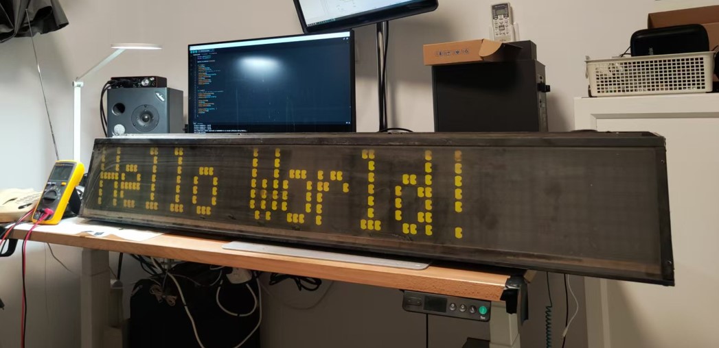
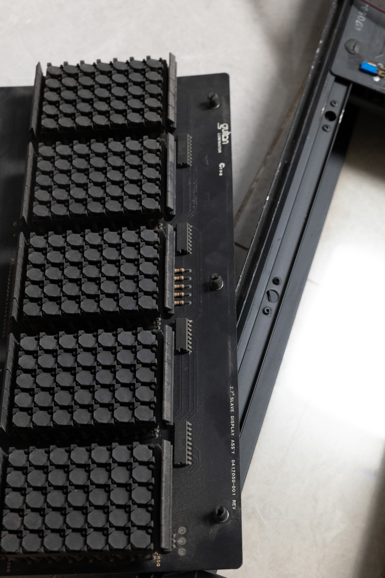
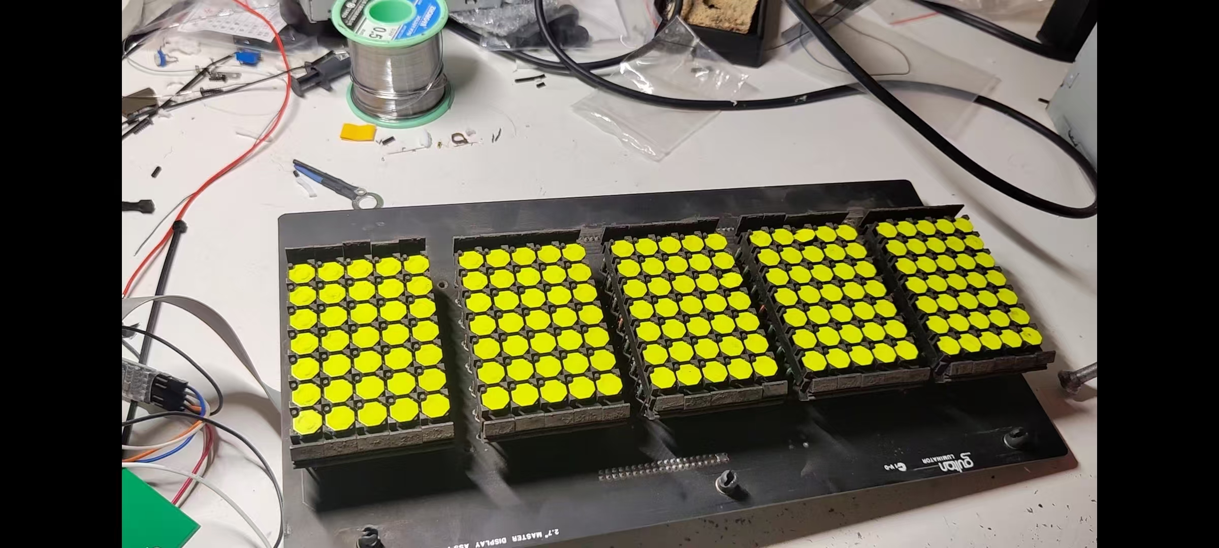
The set of rollsigns I got were made around 1988 to 1990. They are the Gulton Luminator Max: 15 characters 5×7 display.
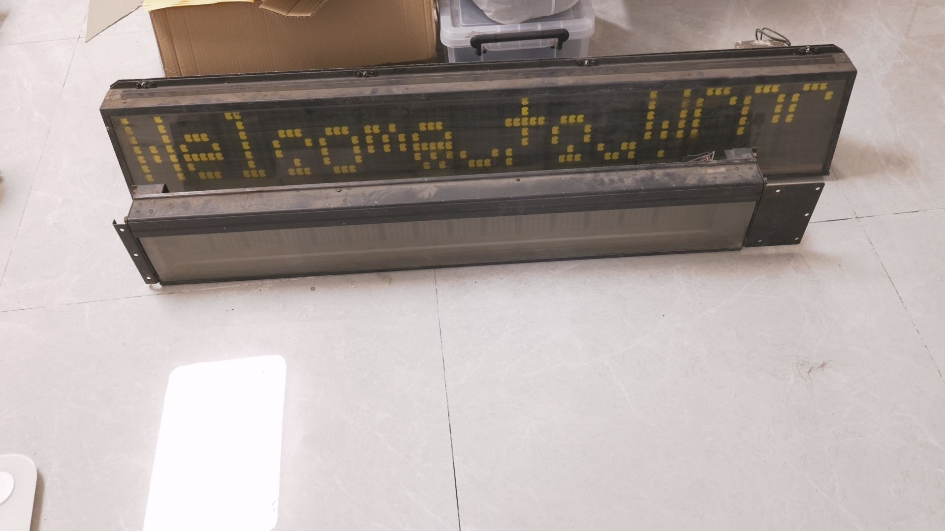
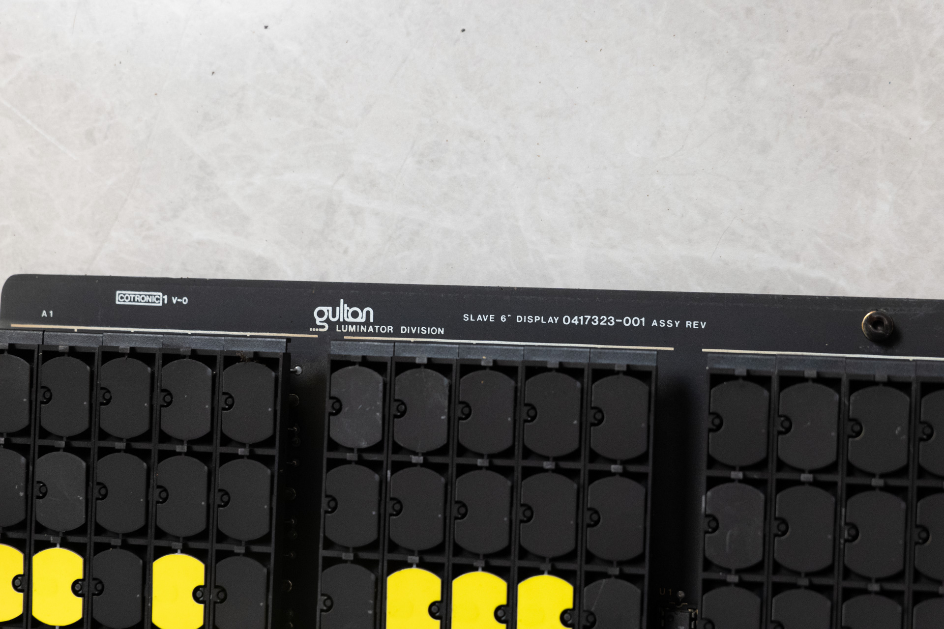
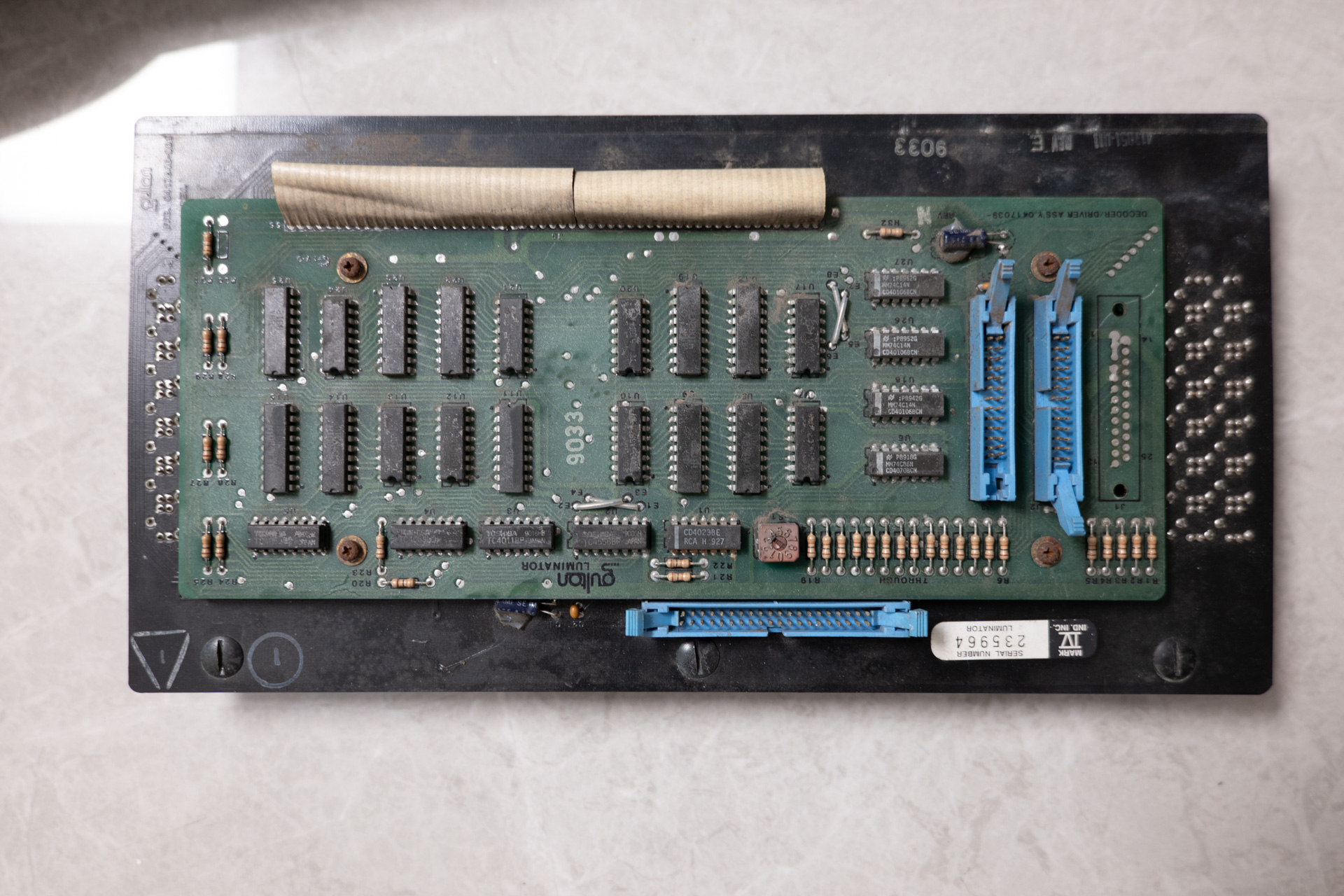
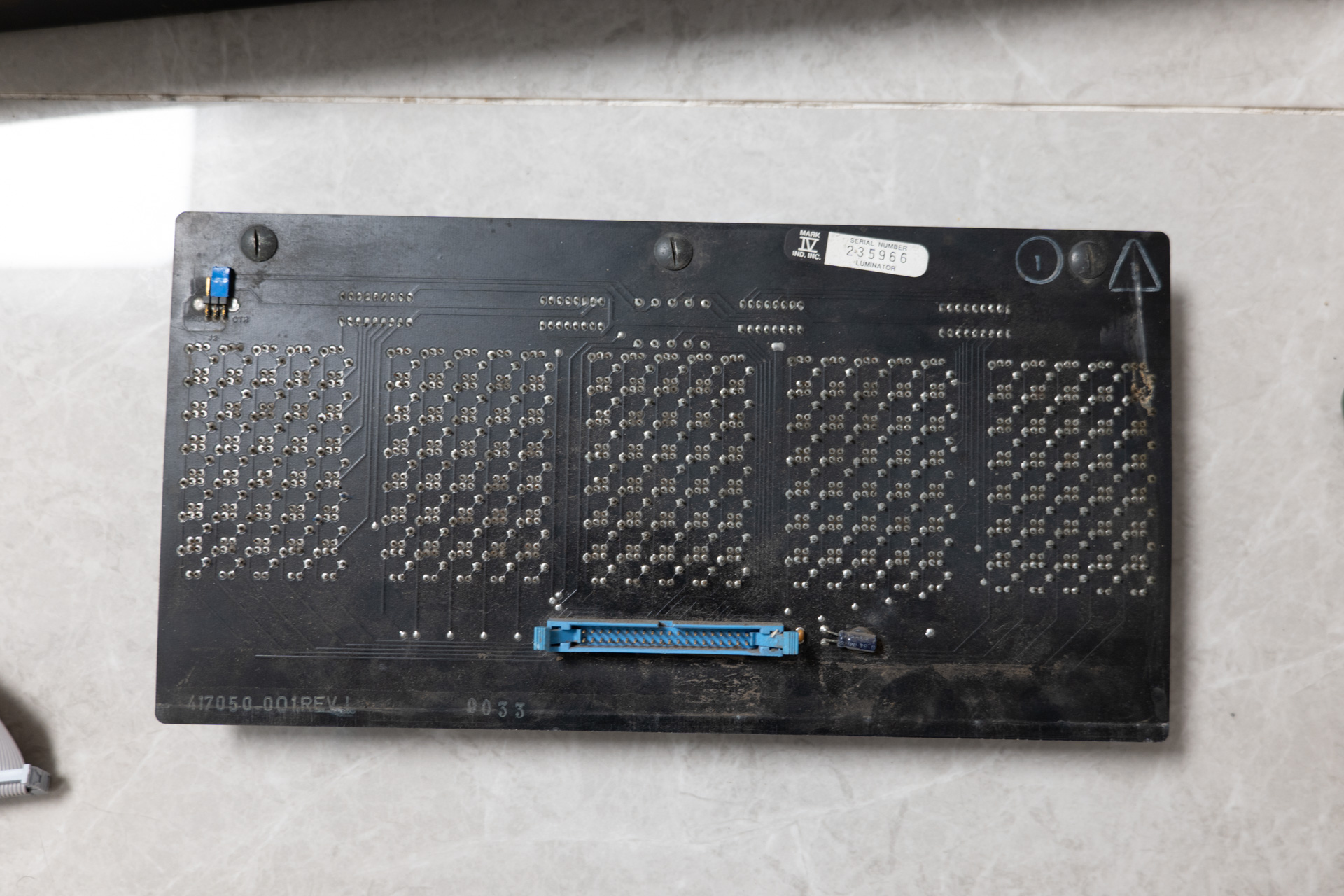
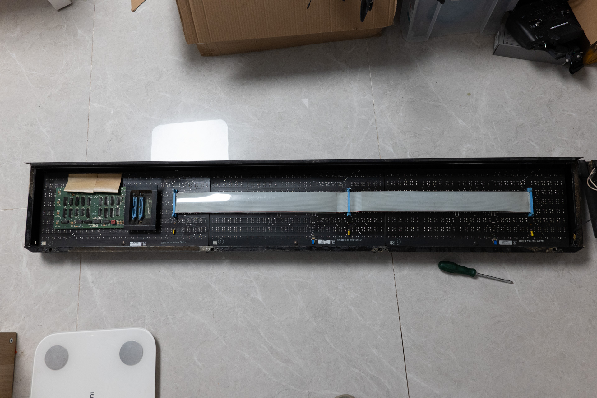
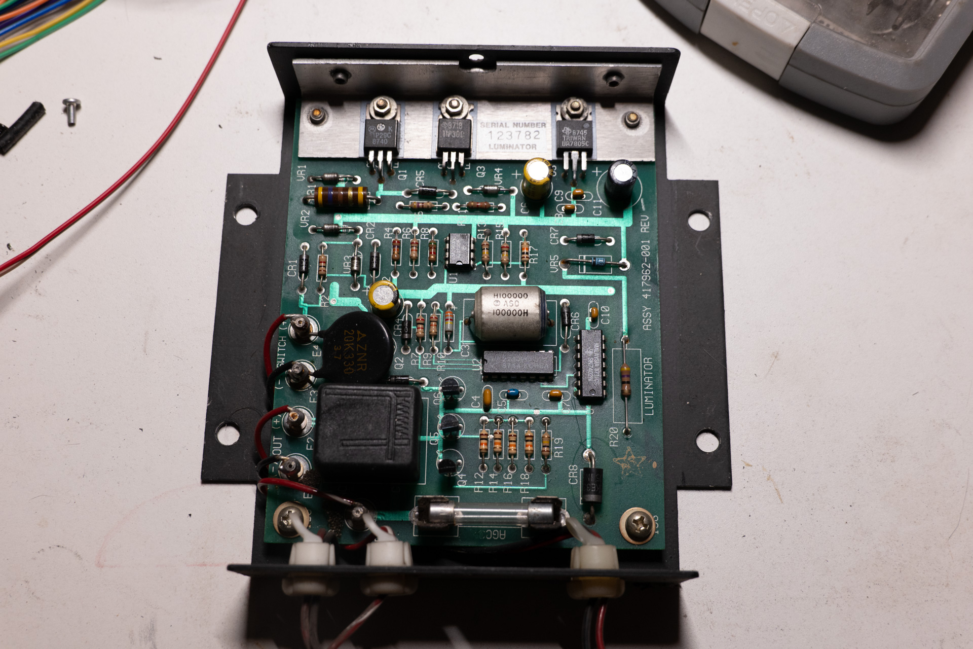
Each display has 3 module boards, one master module and 2 slave module. Between the front large display and the smaller side display, they seem to only differ in size, but identical in circuit design. The master module contains a driver board which accept signals from a control console.
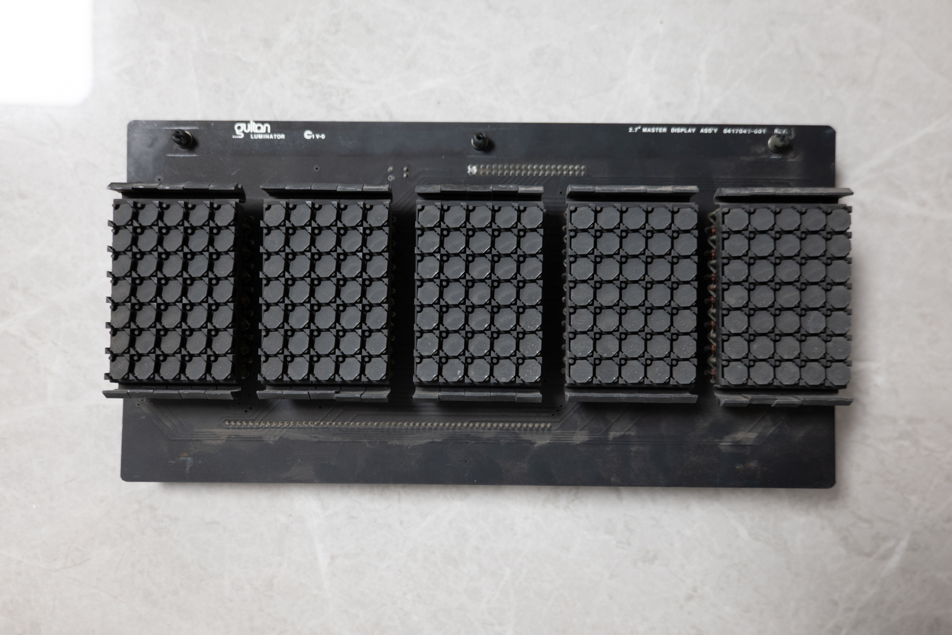
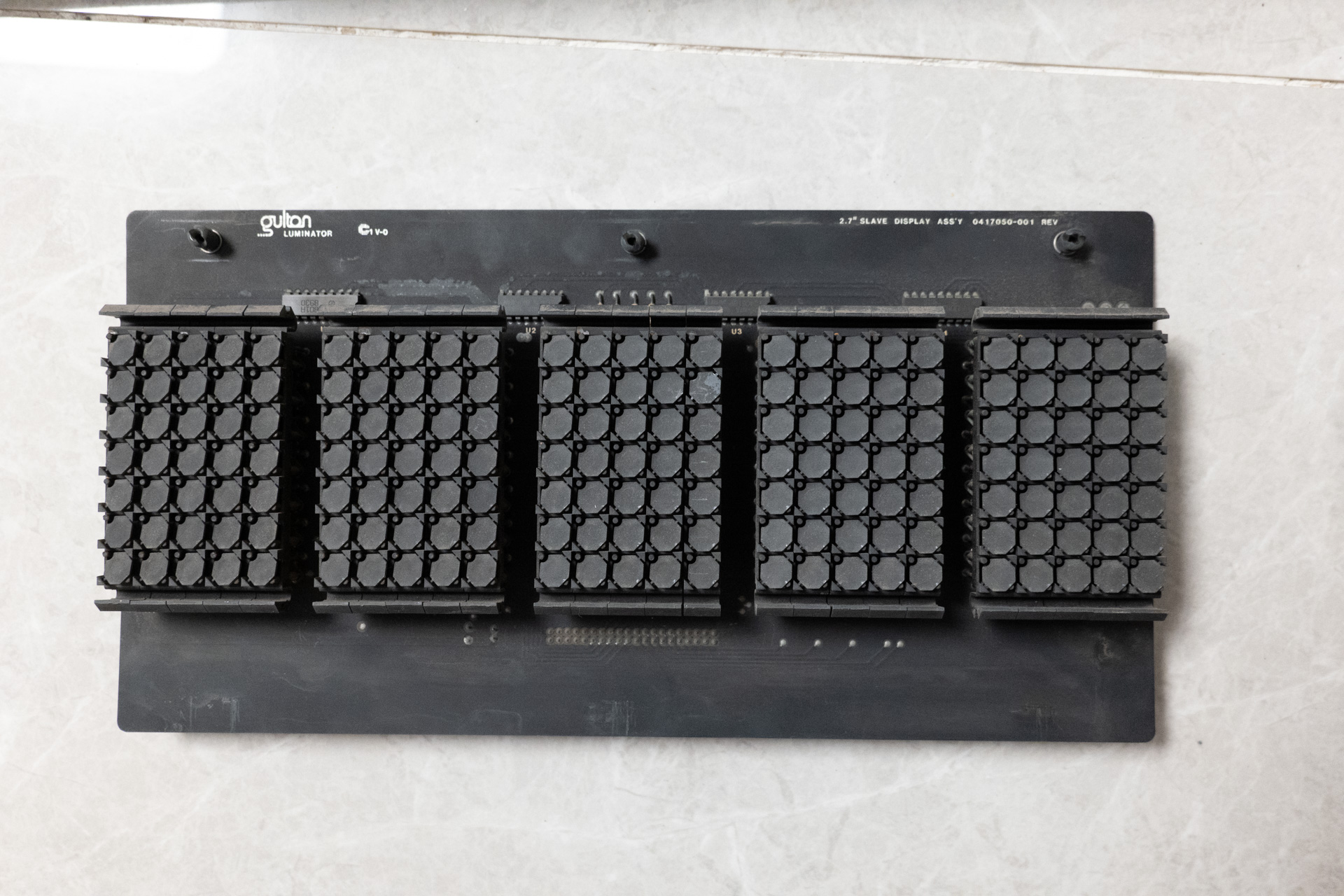
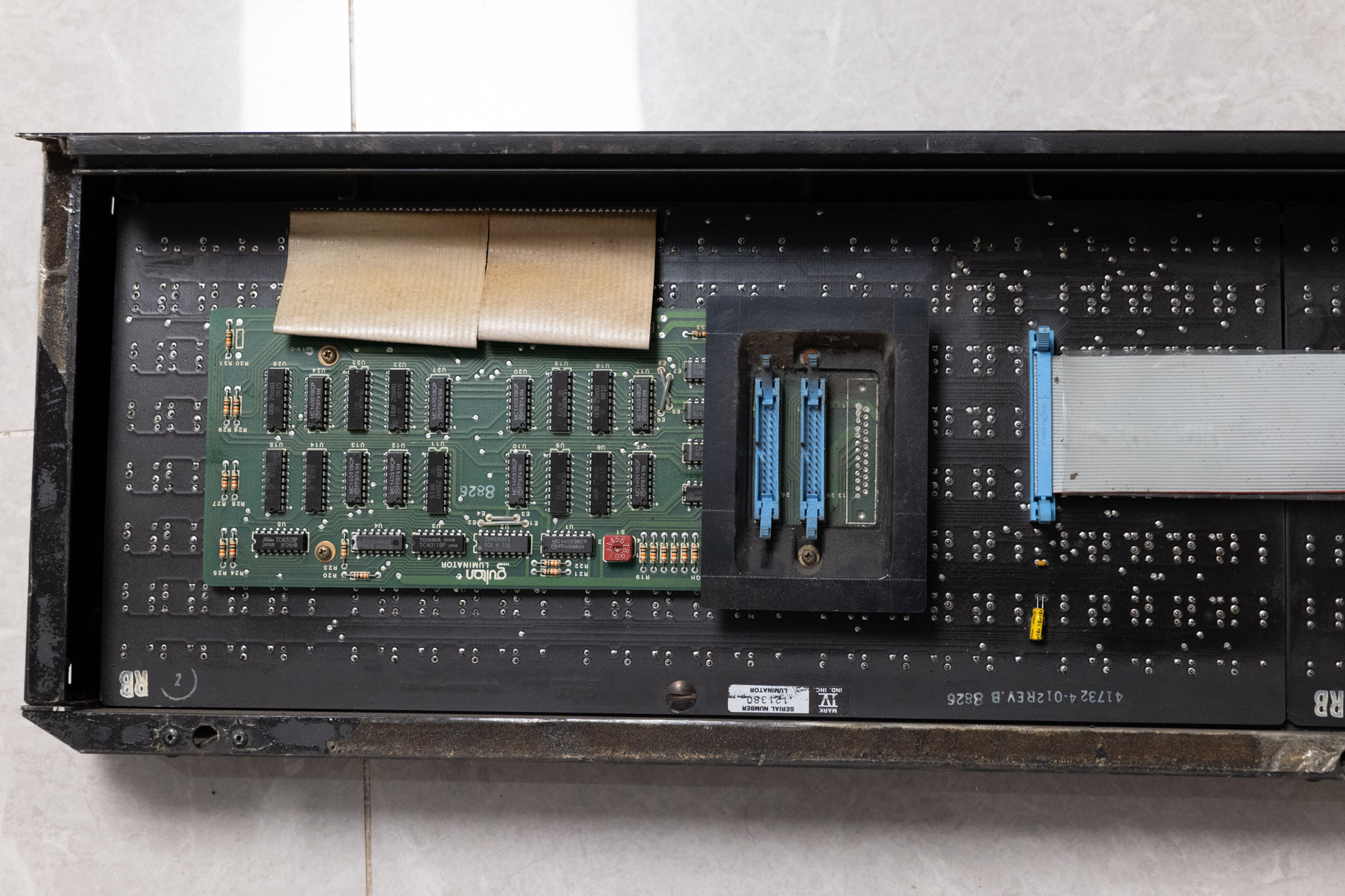
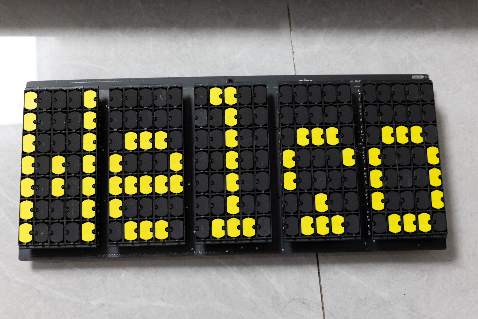
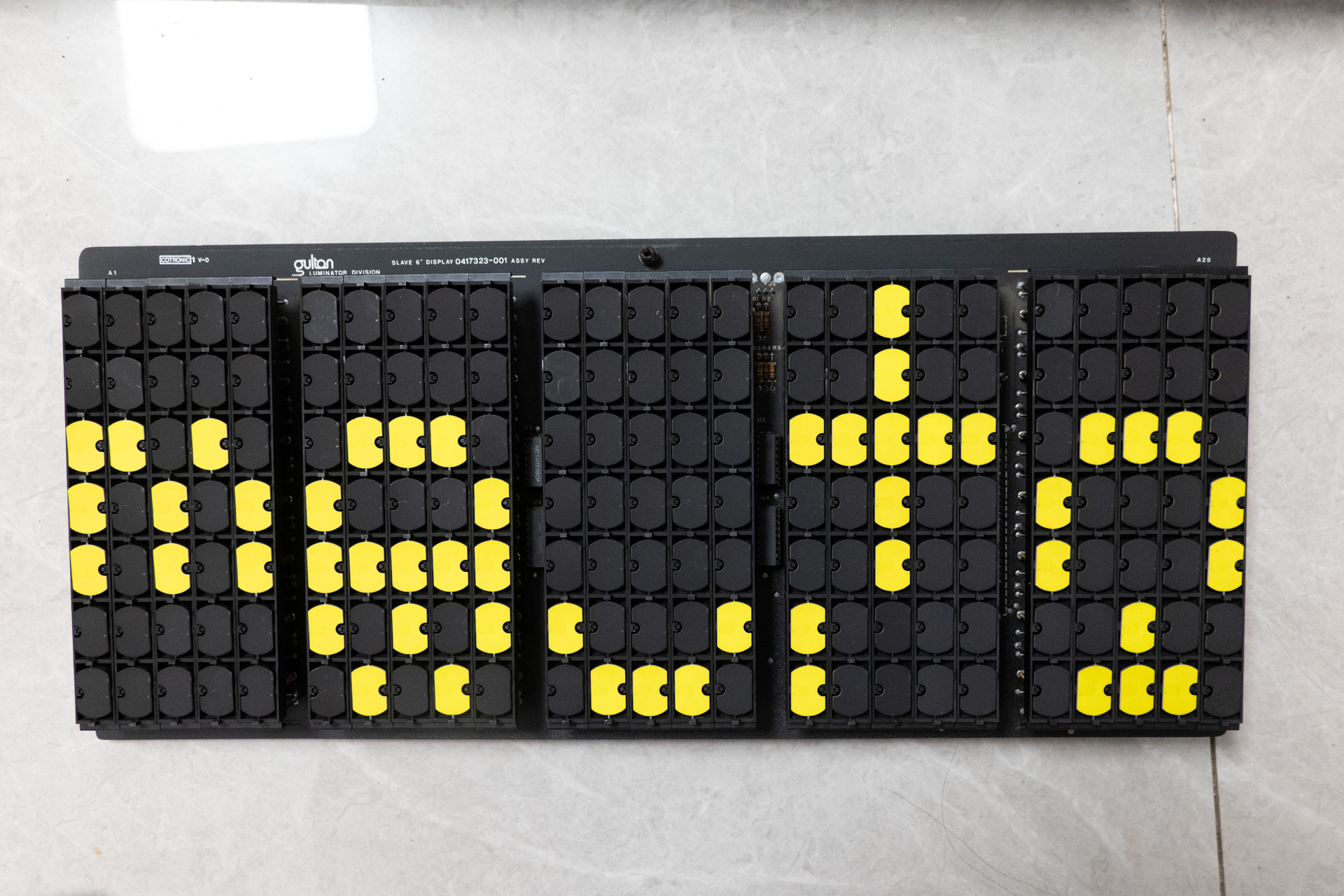
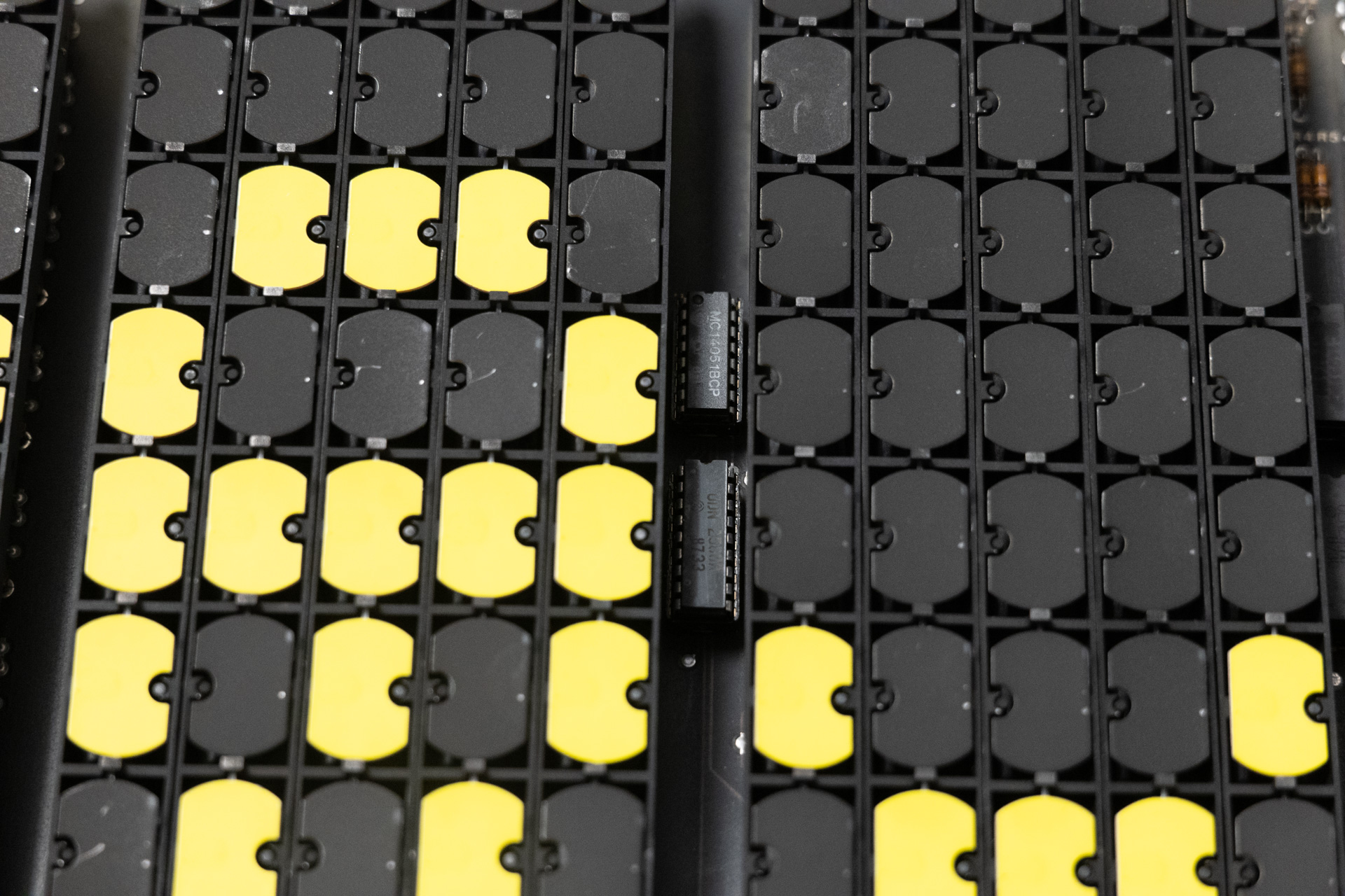
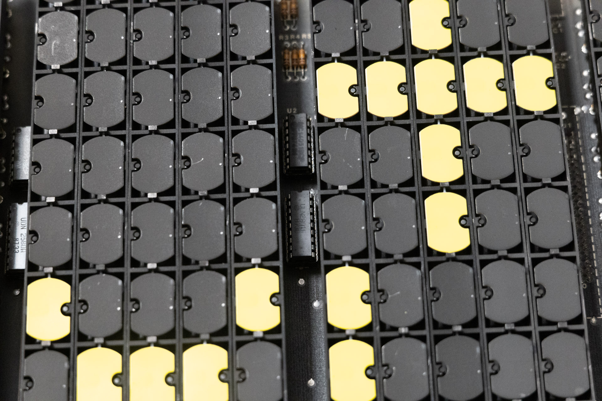
Each module contains 5 characters of 5×7 pixel flip-dot elements.
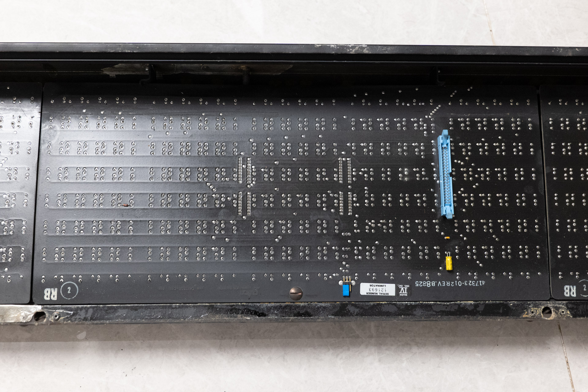
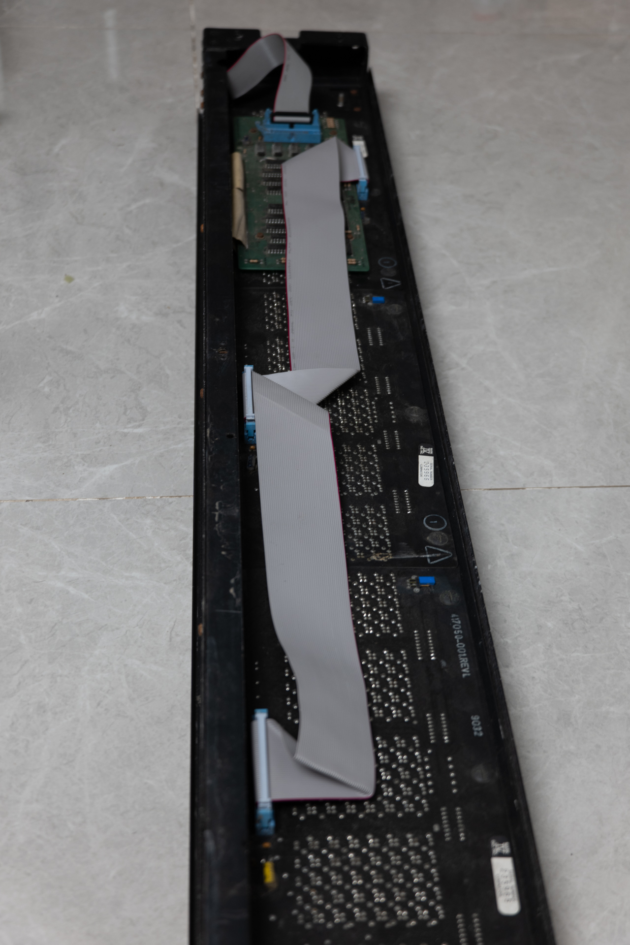
The module boards are connected together with a 40-pin ribbon cable and should be connected to the console with a 26-pin ribbon cable.
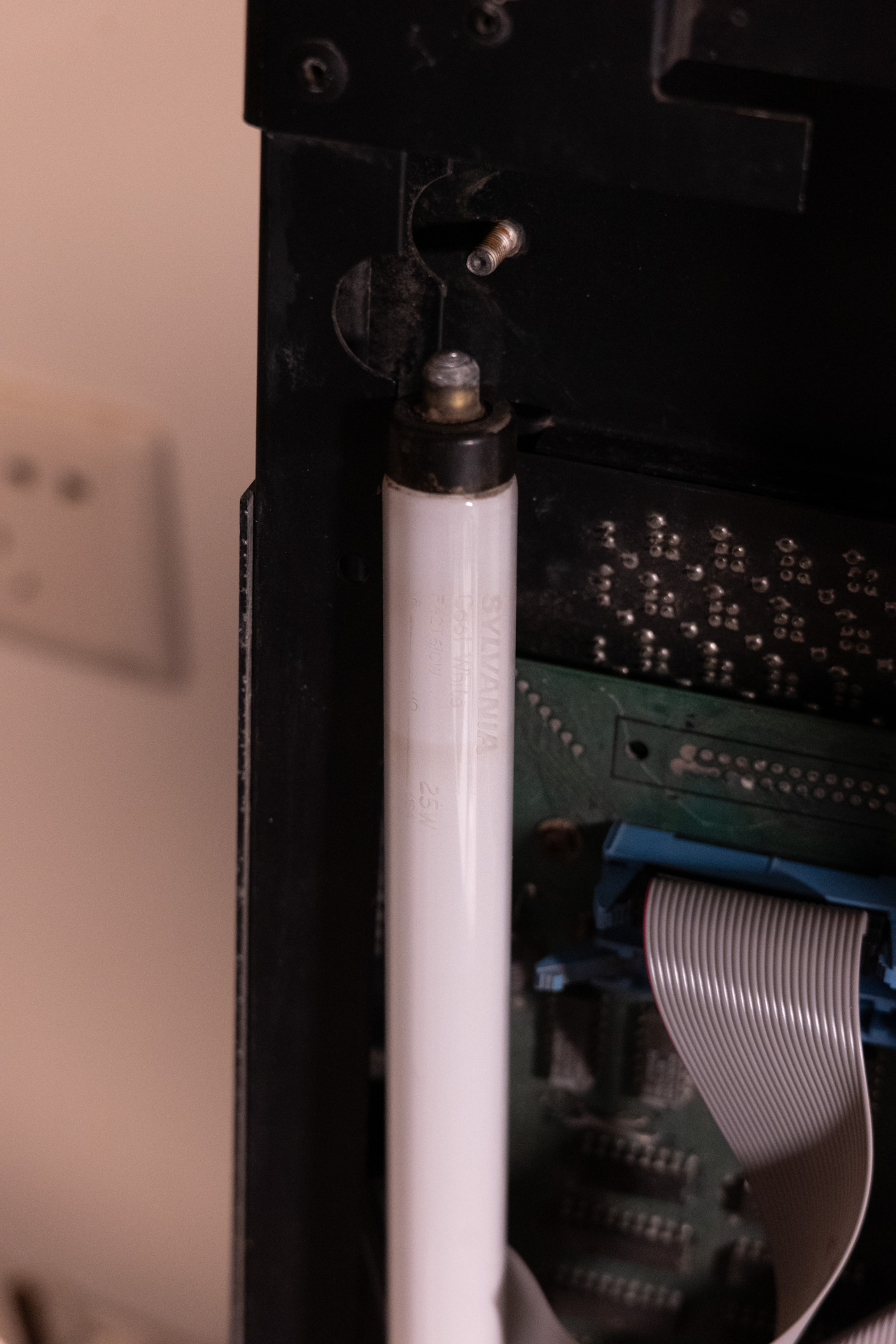
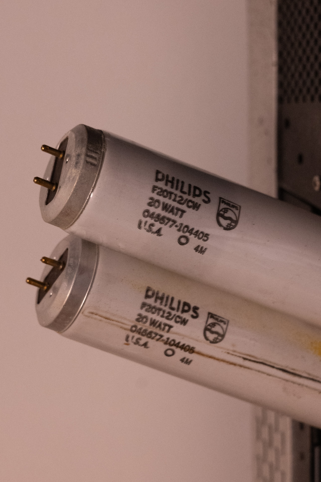
The side display use a single-pin fluorescent light SYLVANIA: F42T6 while the font display use 2 standard fluorescent light F20T12.
They should be equipped with a ballast driver which is a constant current controller for the DC ballast. On my set only the front display came with one.
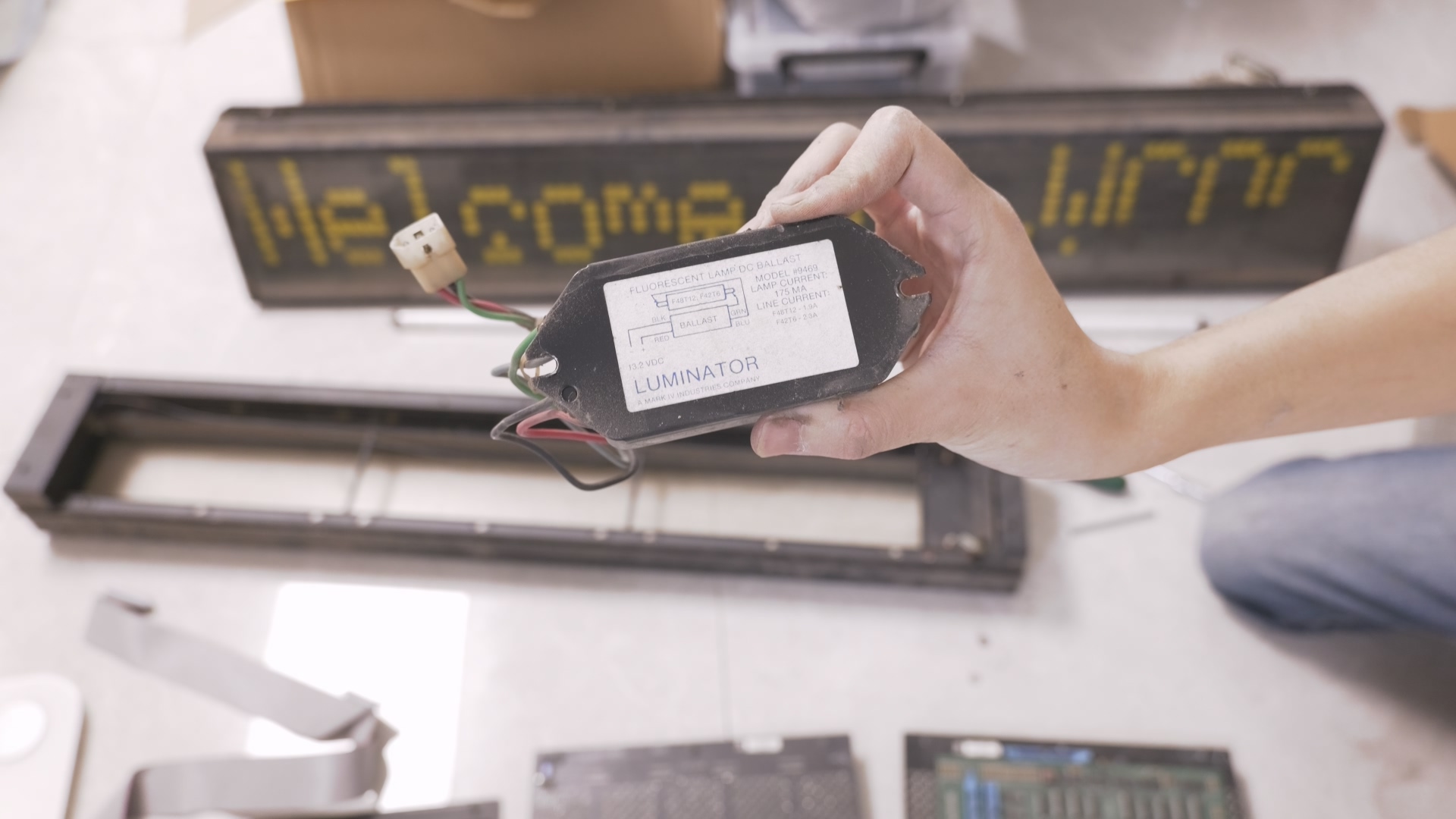
Each vehicle should be equipped with a display control console. The seller didn’t include one. In the original setup, changing of pre-defined display content is done by either swap out (E)EPROMS or by using MTU device (on certain models).
Flip-dot Display
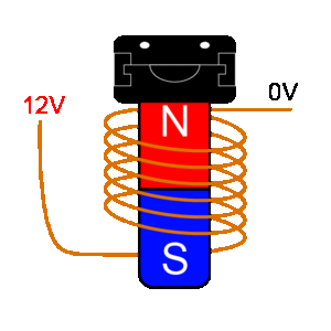
The flip-dot display is a kind of electro-mechanical display often used during 1960s to 2000s, and still used today for art installations. It’s often used for large format displays as it’s very energy efficient (like E-Ink display, only consumes power when changing display content). It’s also the only viable solution for many signage displays before LEDs were widely available and reliable enough.

The flip-dot element use an electro-magnet with a core to control the disc orientation. There is a small permanent magnet embedded in the disc. Once the core is magnetized in one direction, the disc can stay in that side (if the disc is lightweight enough, or if it rotates horizontally). Usually one side of the disc is painted black and the other white or bright greenish-yellow to make high contrast display.

Reverse Engineering of the Master Module
Way of Work
For stuff like this there is usually two ways to re-use them, one is to strip them down to bare minimum and keep only the actuators(in this case, the flip dot elements), or the other one is to take advantage of as much of the electronics as possible. For this project I chose the later, to reverse engineer the circuits. It will be hard and time consuming to make driver circuitry for hundreds of elements.
Board Overview
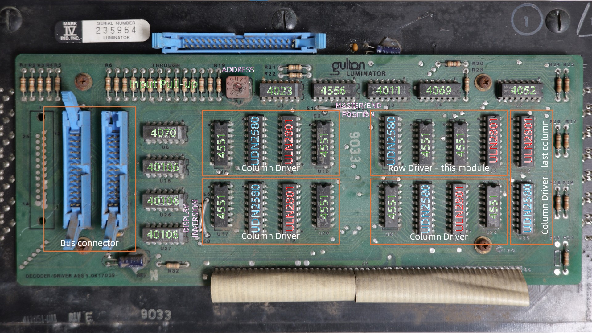
The flip dot solenoids require bi-polar driving to inverse (flip) its magnetic field, which means it requires H-bridge style driver circuit. There are ULN2801 high side drivers and UDN2580 low side drivers on the board and they are arranged in pairs. Each driver chip is controlled by a connected 4551. By just looking at the board and do some counting we can assume that there is one section dedicated to row driving(7 rows) and the rest for column driving. The number of column 25 is somewhat embarrassing, if it were 24 it will be perfect(it can be divided by 8). so there are extra pair of drivers.
There is a rotary switch, obviously for address. There are hex inverters near the bus connector. There are some other logic chips. Everything is 4xxx CMOS, which means there is only one supply rail and it’s shared between logic and driving of solenoids.
The slave boards have their own row drivers.
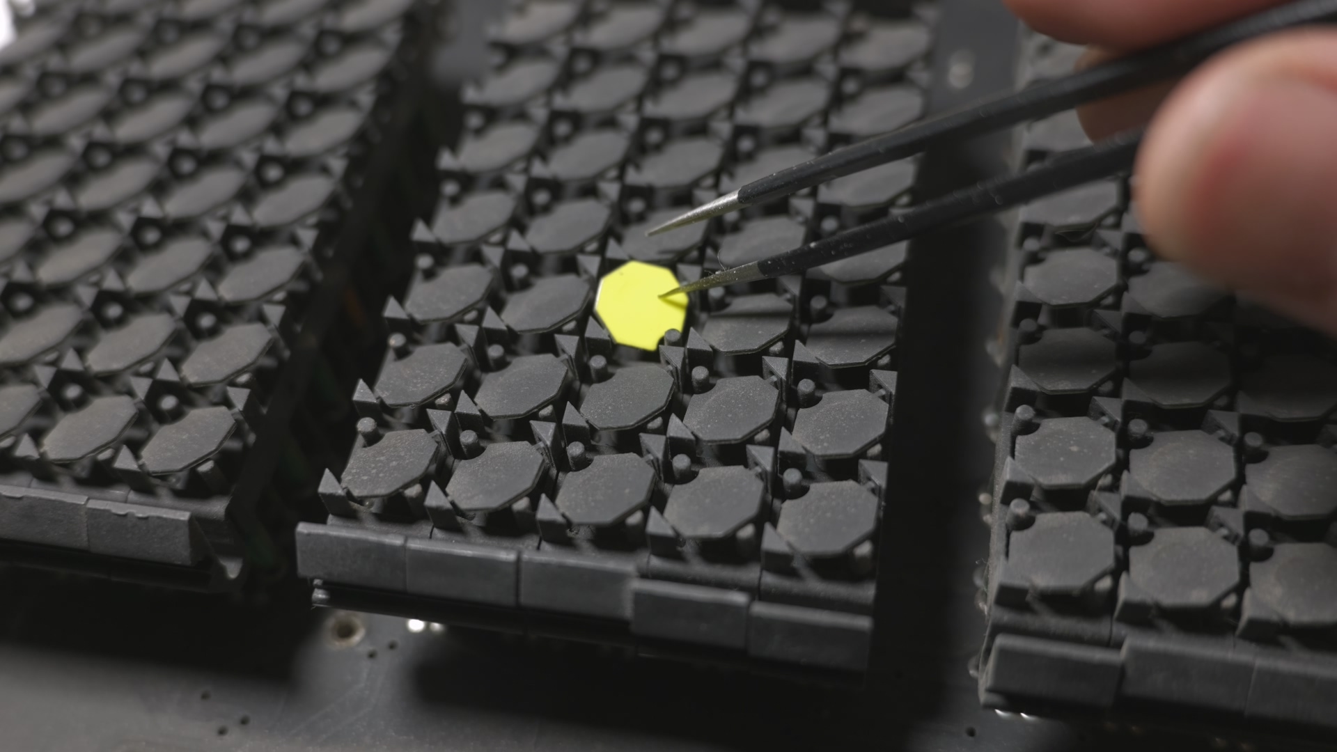
By using a multimeter in continuity mode we can map out the circuit diagram. A small copper brush connected to one side of the multimeter can be very useful. As it is all DIP packages, it’s fairly easy. Although you may want to clean the board and use some chemicals to remove oxidation before working on it.
Reverse Engineer of Circuit
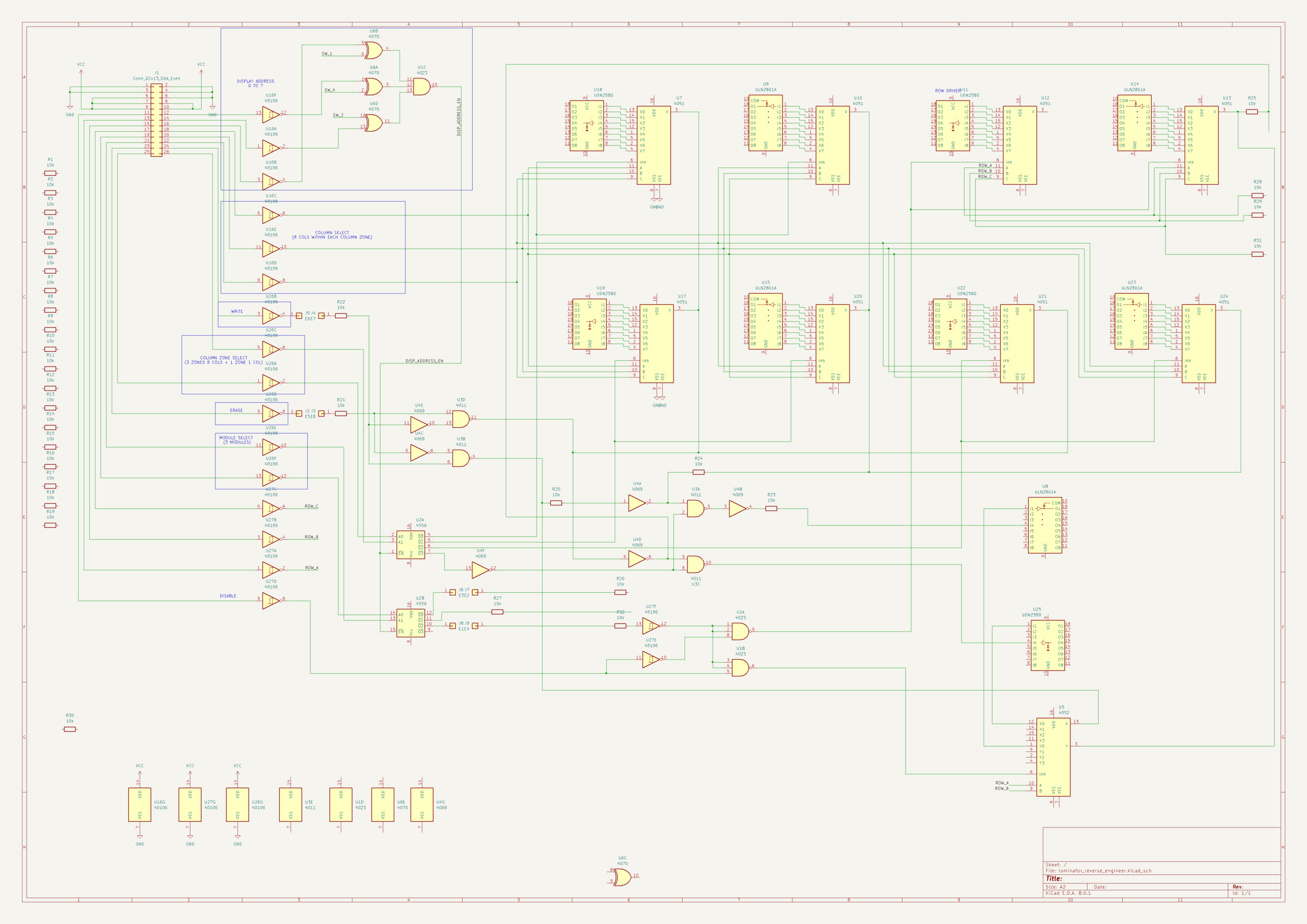
Signals coming from the bus connectors are pulled-up by 10K resistors, and fed into inverters used as bus receiver. On the bus cable it’s active low and in the board after the inverters it’s active high.
The 3 address signals are compared with the rotary switch using 4070s and 4023 to generate an enable signal.
2 column zone selection signals are fed into half 4556 multiplexer to select 4 column zones (3 zones of 8 columns + 1 zone of 1 column), the 4556 output Qs control both high and low side drivers by controlling the inhibit pin of the corresponding 4551 multiplexer. 3 column select pins are connected to the input of 4551, they select single column in the first three 8 column zones, completing all column select circuitry.
2 module select signals are fed into half 4556 multiplexer to select 3 modules(master, middle and end), the output ultimately control the inhibit pin of the 4551 which is connected to row drivers. The 4th Q of 4556 is not used. There are jumper wires to select which module connect to Q0 and which to Q2, so it’s possible to mount the master module on either left or right side.
3 row select pins are connected to the 4551s which control row drivers.
Erase and write pins are logically connected to be exclusive and ultimately control the common pin of the 4551 multiplexers. Erase and write signals have jumper wires so that they can be inversed, which inverse the display in hardware.
A disable pin is provided, it works by controlling row driver.
So now we can have pin definitions (pin number is in odd-even numbering, on external interface all digital signals active low, CMOS level, with regard to VCC):
| Pin Number | Pin Name | Pin Function |
|---|---|---|
| 1, 2, 3, 4, 6 | GND | Negative supply, vehicle chassis |
| 5, 7, 8, 9, 10 | VCC | Power supply |
| 16 | !ADDR0 | Address pin, compared with rotary switch output bit 0 |
| 14 | !ADDR1 | Address pin, compared with rotary switch output bit 1 |
| 12 | !ADDR2 | Address pin, compared with rotary switch output bit 2 |
| 18 | !COL0 | Column select pin, connected to column 4551 input “A” |
| 20 | !COL1 | Column select pin, connected to column 4551 input “B” |
| 22 | !COL2 | Column select pin, connected to column 4551 input “C” |
| 24 | !WRITE | Pull low to set dot to yellow side |
| 23 | !ERASE | Pull low to set dot to black side |
| 25 | !COLZONE0 | Column zone select pin, connected to 4556 input “A0” |
| 26 | !COLZONE1 | Column zone select pin, connected to 4556 input “A1” |
| 19 | !MODULE0 | Module select, connected to 4556 input “A0” |
| 21 | !MODULE1 | Module select, connected to 4556 input “A1” |
| 13 | !ROW0 | Row select pin, connected to row 4551 input “A” |
| 15 | !ROW1 | Row select pin, connected to row 4551 input “B” |
| 17 | !ROW2 | Row select pin, connected to row 4551 input “C” |
| 11 | !DISABLE | Pull low to disable whole system |
Reverse Engineer of Timings and Voltages
The patent of the Luminator system is available online so it can be used to get a lot of useful information and also to confirm we have done the correct reverse engineering. It’s located at https://www.freepatentsonline.com/EP0090043.pdf
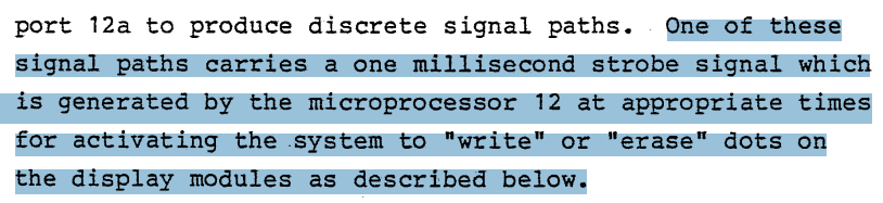
From the patent, we can know that the console sets the address, row, columns and then toggle the WRITE or ERASE signal for a given pulse length to set the display. This pulse length is critical, if it’s too long you risk frying the coils and if it’s too short the display may not be set correctly. In the patent, the pulse length is 1ms, which we can use as a baseline. If you are testing similar flip dot display boards, you can put a high-pass filter in series in the pulse signal. This way even if your controller is giving too long a pulse or straight voltage level, the coils won’t be damaged.
The voltage to power the boards however is not mentioned. Base on my experience and the logic chips used, I think 9 to 15V is a valid range. And further test shows that this range works well, with 9V on the weaker slower side but also provides quieter operation. I decided to use 12V to power the system.
Making the Displays Work
Restoration
The smaller side display is missing the 40-pin ribbon cable that connects the module boards together, as well as the back cover. I crimped a new 40-pin IDC cable with 3 connectors (very similar with IDE cable).
All of the modules in the side display are extremely dusty. This does not affect operation but will impact display contrast. I cleaned all of the modules using a soft brush. I washed all of if with pure alcohol.
I’ve designed a new back cover for the side display but has yet to manufacture it. I’ll replace the fluorescent lamps with COB LED strips.
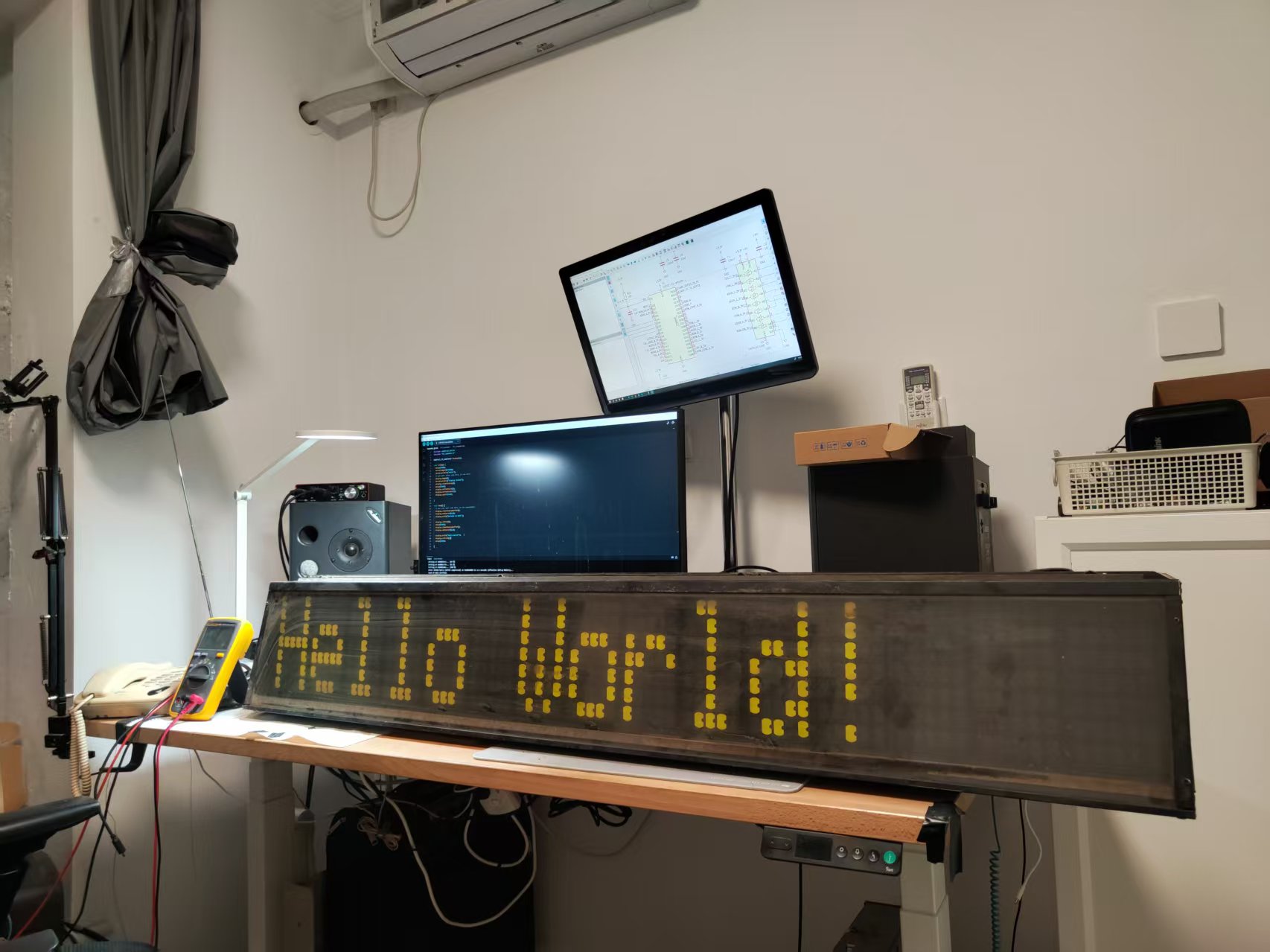
New Controller Board
With the reverse engineer result we can now design a new control system for the displays. I want to use one board to control both (or more) displays, with the ability to remotely alter the display content.
Hardware
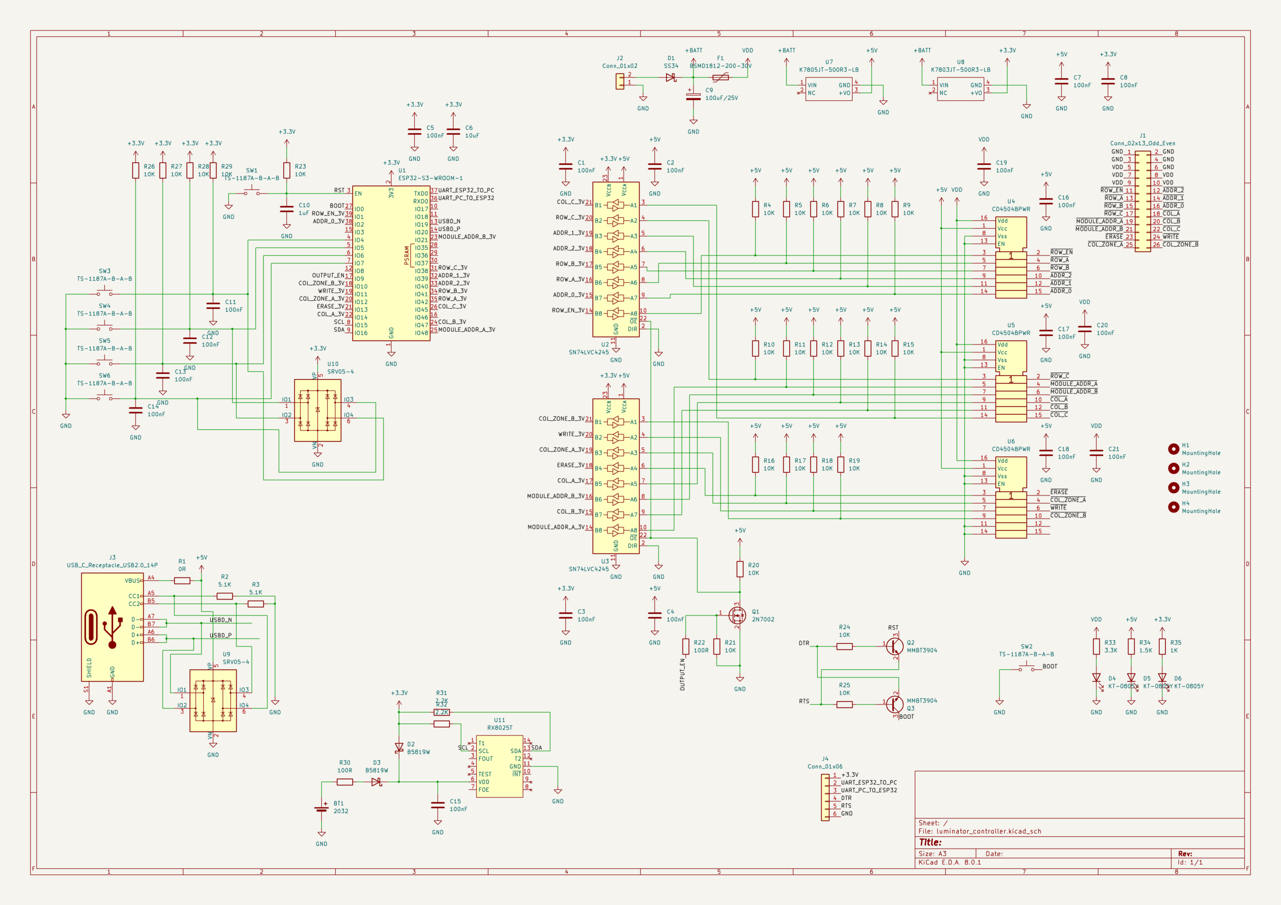
I designed a board using ESP32-S3 Wroom module as main controller. The ESP32 modules are leftover material from the SRJV project. There are two sets of level shifting circuits, it first shifts the 3.3V level from the MCU to 5V using 74LVC4245, then it shifts from 5V to CMOS level (9 to 15V) using CD4504. The board also include 5V and 3.3V power supply, utilizing MORNSUN buck converter modules (I did it the lazy way this time). I put 4 buttons on the board, a RTC chip, a CR2032 battery holder, USB circuitry for ESP32, and the auto programming circuit for ESP32. Some basic protection circuits were included.
I manufactured the board at JLCPCB and have the SMT done partially. I usually do this to balance between cost and the time and effort I have to put into soldering components. The board came back nicely and it works no problem.
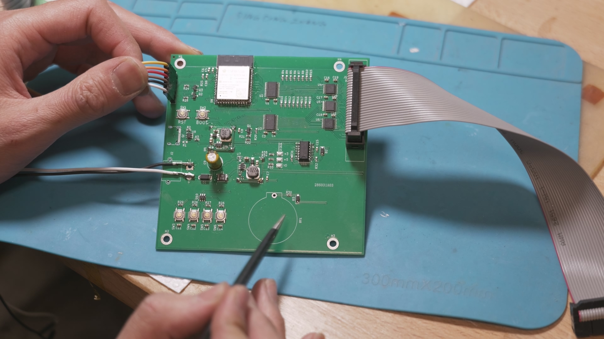
I crimped 26-pin IDC cable to connect the board to the display, initially one at a time. I tested the board and the display with some simple program, like dot-by-dot writing, and everything works fine. The displays have no dead dot either.
Software
I used Arduino IDE to write the firmware for the controller board. I initially was deciding between Adafruit GFX, LVGL and U8g2. I finally set the target to make a custom driver for this display for Adafruit GFX as it’s lightweight, versatile and simply being used a lot.
Display arrangement
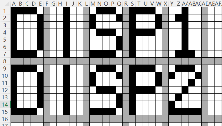
The actual displays are 5x7x15, with about one pixel spacing between each character. So I set the display area of each character to (5+1)x(7+1), which can simplify a lot of things, as the built-in display font in GFX is 5×8 in size and 1 pixel spacing. When writing the pixels, every 6th column is discarded.
The driver class takes a parameter of display numbers. If initialized with more than 1 display, the displays are arranged vertically. When writing the pixels, every 8th row is discarded.
Pixel Buffering
In the original patent the display is refreshed pixel by pixel, suggesting some kind of single buffering (or no buffering). I implemented both single buffering and double buffering in the driver class. As this display has no memory, the graphics memory need to be on the controller side. Double buffered refreshing is usually significantly faster than single buffer, as we can compare the content to display next and what’s on the display, and only change the dots that need to be flipped. For flip-dot display this is very important as the refresh speed is so slow (~1ms per pixel).
Font
The Adafruit GFX built-in font is actually 5×8. for the lower case alphabets I had to make some modification to make them appear complete in the flip-dot display.
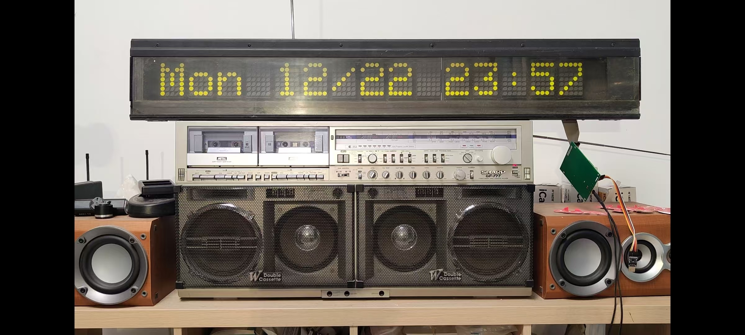
Current Usage
I’m currently using the side display as a clock. However it’s a bit too noisy. I may fix the larger front display on the wall and use that to display stuff that need more updates. The larger display is actually quieter.
Other things can be displayed, like weather forecast, 3D printing status, news feed, etc. It’s just some software coding, all the infrastructures are already there.
Hi!
Great job! I have a display like this one (just the front one) and started doing the reverse engineering a few years ago but never finished… Your work will help me a lot.
Thank you for the great and detailed article.
Hello how are you? i want to know how much cost me the card wi fi for my jv1080 with dhl shipping to country : argentina , state: buenos aires , zip: 7600
thanks a lot!!!
Hi:
I’ll use another express service provider. The standard shipping cost $6 apply. You can purchase as normal.
Hello! nice to meet you, here in argentina the only one that can deliver the product withot problema is Dhl , can you ship with Dhl? please?
Hi:
I have no control over the last-mile-delivery provider and I cannot ship via DHL. However if you can’t receive the product due to delivery issue, you can have a refund.